While chip makers fight for attention with ever-bigger GPUs and AI breakthroughs, one low-profile Japanese group quietly holds the keys to production. Without its thin, beige-looking film, most high-end chips for data centres, laptops, cars and game consoles simply could not be assembled.
From soup seasoning to strategic tech supplier
For most Japanese consumers, Ajinomoto means supermarket staples: instant noodle broths, seasonings, and the infamous MSG that shaped 20th‑century food culture. Behind these familiar products stands a sprawling industrial group with billions in annual revenue and deep roots in chemistry and fermentation.
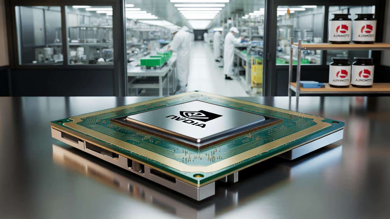
That chemistry expertise, accumulated over more than a century, is what now links grocery aisles to Nvidia’s most advanced AI accelerators. The company has become the near-exclusive supplier of a material called Ajinomoto Build‑up Film, or ABF, a specialised insulating layer built into the substrates that carry top-end CPUs and GPUs.
ABF is a thin insulating film hidden inside chip packages, yet it can halt production for giants like Nvidia, AMD and Broadcom when supplies run short.
Ajinomoto today supplies about 95% of global ABF output, according to industry estimates. That gives one Japanese food-and-chemicals group an outsized influence over the pace of AI deployment worldwide.
The unlikely origins of a chip bottleneck
Umami, glutamate and a century-old gamble on chemistry
The story starts in 1908, long before clean rooms and EUV machines. In Tokyo, chemistry professor Kikunae Ikeda became obsessed with the deep, savoury taste of his wife’s kelp soup. By isolating glutamate from seaweed, he identified a fifth basic taste that would later be known as umami.
Ikeda moved fast. In 1909, he founded Ajinomoto—literally “the essence of taste” in Japanese—to produce and sell monosodium glutamate as a flavour enhancer. To scale up, the company invested in fermentation, industrial chemistry and biological processes, laying scientific foundations that went far beyond food.
For decades, Ajinomoto focused on amino acids, sweeteners like aspartame, and food ingredients. No one imagined those same labs would later solve a problem that Silicon Valley’s biggest names could not crack on their own.
Waste streams that turned into a strategic asset
During the 1970s, Ajinomoto’s amino acid plants generated large amounts of chemical by-products. Treating or disposing of them cost money and brought little benefit. Instead of treating this as a pure compliance issue, the company’s scientists began analysing these residual compounds.
➡️ Der psychologische Grund, warum wir uns vor leeren Seiten fürchten – und wie du ihn überwindest
➡️ Diese unterschätzte Routine verbessert Fokus ganz ohne Aufwand
➡️ Der geniale Hoteltrick: So werden Duschwände mühelos streifenfrei sauber und wieder kristallklar
➡️ Die 10 Gemüse, die Nässe besser wegstecken und trotz Regen reiche Ernten liefern
They noticed something striking. Certain molecules showed excellent electrical insulation, impressive heat resistance and stable mechanical behaviour. That made them intriguing candidates for advanced materials, even if no clear market existed yet.
The insight sat in the background for years. Only when chip design hit a physical wall in the 1990s did it become truly valuable.
When Intel’s miniaturisation hit a wall
1996: traditional materials stop keeping up
By the mid‑1990s, Intel and its rivals were shrinking transistors and wiring at a frantic pace. As the metal traces on chips and packaging moved closer together, tiny defects in insulating layers caused serious reliability and yield problems.
Conventional insulating “inks” that were printed and cured on substrates started to fail under these pressures. Manufacturers reported air bubbles, uneven drying, chemical contamination and random failures. At the volumes they were pushing, that meant lost revenue and lost leadership.
Somewhere in the semiconductor supply chain, a materials engineer pointed toward Ajinomoto and its unusual film candidates. The question to the Japanese company was simple but demanding: could they provide a continuous, ultra-clean insulating film that could be laminated and laser‑patterned with near-perfect control?
In less than four months, Ajinomoto transformed waste‑stream chemistry into a high‑precision electronic material that the rest of the industry still struggles to match.
A film nobody else could quite replicate
Ajinomoto took the challenge. The company pulled together chemists, process engineers and materials scientists. Within months, it had a product that changed chip packaging permanently: Ajinomoto Build‑up Film.
ABF is not an ink but a very thin polymer film applied directly on the substrate that sits beneath the silicon die. It offers:
- stable performance at temperatures well above 200°C
- extremely fine laser patterning without warping or cracking
- compatibility with copper wiring and advanced metallisation
- reliable insulation at ever‑shrinking geometries and high signal speeds
Each new chip generation forces tweaks to ABF—thickness, heat behaviour, chemical mix and processing steps all need retuning. That constant co‑development with chipmakers has built a technical moat around Ajinomoto’s product line that newcomers find hard to cross.
How ABF underpins Nvidia’s AI surge
AI chips are no longer just slabs of silicon
Modern AI accelerators pack enormous processing power and memory bandwidth into a tiny footprint. A single Nvidia GPU for data centres combines a massive die with stacked high‑bandwidth memory (HBM) chips, all interconnected through an advanced packaging technique.
At Taiwan’s TSMC, many of these chips use a process known as CoWoS, short for chip‑on‑wafer‑on‑substrate. In broad terms, the GPU and its memory sit on a silicon interposer, which is then mounted on a substrate made of multiple build‑up layers.
Those build‑up layers rely on ABF as their insulating medium. The film must route thousands of ultra‑dense electrical connections, carry high currents, and tolerate repeated heating and cooling without cracking or delaminating.
Remove ABF from the equation and the most advanced AI chips—from Nvidia to AMD and beyond—simply cannot be packaged at scale.
Even Nvidia’s latest architectures, designed for so‑called “agentic AI” that chains together complex reasoning steps, lean on ABF‑based substrates. The computational breakthrough rests on a very physical support layer made in Japan.
A global chokepoint hiding in plain sight
With roughly 95% market share in ABF, Ajinomoto has become a single point of failure in the semiconductor packaging chain. There is no large-scale equivalent plant in the US or Europe, and only limited production in other parts of Asia.
The risk became visible during the 2021‑2022 semiconductor crunch. While headlines focused on chip shortages and lithography tools, some delivery delays stemmed from constraints in ABF supply. Companies such as Broadcom saw product lead times stretch past 70 weeks, not because of missing silicon, but because the substrates underneath could not be produced fast enough.
| Stage | Key dependency | Typical geography |
|---|---|---|
| Chip design | EDA software, IP blocks | US, Europe, Taiwan |
| Wafer fabrication | Silicon, lithography tools | Taiwan, South Korea, US |
| Packaging & substrates | ABF insulating film | Primarily Japan (Ajinomoto) |
This kind of bottleneck is hard to fix quickly. Building a competing ABF line requires not just capex, but also decades of know‑how in polymers, process control and co‑development with chipmakers. For now, Ajinomoto’s grip looks resilient.
AI demand is driving Ajinomoto’s next growth wave
Ramping capacity for a hotter, denser future
Ajinomoto plans to expand ABF capacity by around 50% by 2030, according to industry projections. Global demand grows near double digits annually as AI accelerators spread from cloud data centres to automotive, networking gear and high‑end PCs.
Each new generation of chips tends to use:
- more substrate area per package
- more build‑up layers to handle added complexity
- tighter wiring, which raises demands on insulation quality
That translates directly into more square metres of ABF rolling out of Ajinomoto factories. As long as AI models keep scaling in size and cost, the company’s electronic materials division should see steady tailwinds.
Why ABF is so hard to replace
Technical, economic and geopolitical hurdles
On paper, making an insulating polymer film might not sound exotic. In practice, ABF combines several conflicting properties that are tricky to balance: ultra‑low electrical loss, precise thermal expansion to match other materials, resistance to moisture, and compatibility with harsh processing chemicals.
Shifting away from ABF also carries massive validation costs. A new material requires fresh reliability testing, redesign of substrate layouts, and fine‑tuning of entire packaging lines. For manufacturers already racing to meet AI server demand, the incentive is to keep using what works.
There is also a geopolitical angle. Governments in the US and Europe are pouring subsidies into fabs, but packaging materials get less attention. A supply disruption caused by natural disaster, export controls or industrial accident in Japan would ripple through AI infrastructure worldwide, from cloud providers to car makers.
What this means for AI, investors and ordinary users
For AI researchers and cloud providers, Ajinomoto’s dominance adds another layer of fragility to an already stretched supply chain. Shortages in ABF would not just raise prices; they could slow rollouts of new GPU clusters and limit access to cutting‑edge models.
Investors who only watch chip designers and foundries miss part of the story. Value accrues not just at the top of the stack but also in seemingly mundane components that gain strategic relevance. ABF sits in the same category as photoresists, advanced gases and EUV optics: obscure to the public, central to the industry.
For everyday users, this hidden dependency will rarely appear on a product spec sheet. Yet it shapes whether a new AI feature is available on your phone this year or next, whether car makers can ship updated driver‑assist systems, and how fast companies can train the next generation of language and vision models.
Two technical terms often used around this topic deserve clarification. A substrate is the multilayer “circuit board” that carries the chip and routes signals from it to the outside world; ABF is one of the thin insulating layers inside that structure. Packaging is the full process of attaching the chip to the substrate, adding connections, and protecting it so it can be mounted on a bigger board.
If AI keeps scaling, demand for clever packaging and specialised materials like ABF will grow alongside model sizes. That places an unassuming film, born from a century-old fascination with flavour, at the centre of the next decade of computing.